
What is an FR4 PCB?
Flame Retardant 4, or FR4, is a material grade used in PCB manufacturing. It is made of fibreglass and “4” represents the UL94 V-0 flammability standard (it must self-extinguish after being ignited). Fibreglass reinforced woven glass fibre and epoxy resin with makes it excellent for electrically insulated applications. FR4 is a widely used material due to its low cost and high reliability.
FR4 Material Overview
FR4 represents flame-retardant grade 4 glass-reinforced epoxy laminate. The material’s dielectric constant and dissipation factor (loss tangent) are moderate. FR4 can be used in low-speed and high-power applications, making it the first choice for many hobbyists. This makes it suitable for general-purpose electronic designs.
Dielectric constant: around 4.5 at 1MHz (moderate). Loss tangent: around 0.02 at 1MHz (moderate). The glass transition temperature (Tg) determines how the material behaves under heat. It is one of the most important thermal properties in the classification of FR4 materials.
FR4 comes in three different temperature ranges:
- Low Tg (130–140°C)
- Standard Tg (150–160°C)
- High Tg (>170°C)
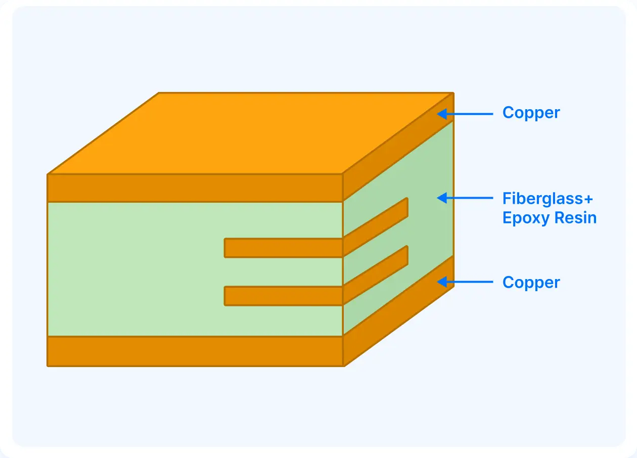
Structure and Properties of FR4
FR-4 is a composite material used as the substrate in PCBs. Its structure is made from:
1. Woven Fiberglass Cloth (E-glass fibers): Fibreglass provides higher mechanical strength and appears as a fine woven fabric inside the laminate.
2. Epoxy Resin (flame-retardant, brominated): Epoxy acts as the matrix, binding the fiberglass together and providing excellent electrical insulation and thermal resistance.
3. Copper Foil (in PCBs): Copper foil layers are used to make tracks and are laminated onto FR-4 using heat and pressure.
Making a PCB – PCB Manufacture Step by Step


Standard PCB
Here at GOJGO, Standard PCB service refers to full feature printed circuit board manufacturing service. With 20+ years’ experience in PCB fabrication, we have handled hundreds of thousands of PCB projects, and covered almost all kinds of substrate materials including FR4, Aluminum, Rogers, etc. This page only touches standard FR4 based PCB. For PCBs with special technical substrate, please refer to corresponding webpages for information.
Get an Instant Quote for Standard FR4 PCB Fabrication
Unlike Prototype PCB service, our Standard PCB service has tighter production tolerances. The following two articles will give you enough information about those two services on their introductions and differences:
- • PCB Prototype & Standard PCB Manufacturing Services Comparison
- • When to use PCB Prototype Service and when to switch to Standard PCB Service
It is recommended to use Standard PCB service when your design is ready to transform from prototype phase to production phase. We can manufacture up to 10 million pieces high quality PCBs in as short as 2 days. To endow your project with expected function and more possibilities, we offer advanced features for Standard PCB services. Comprehensive capabilities can be found in the following table:
| Feature | Capability |
| Quality Grade | Standard IPC 2 |
| Number of Layers | 1 – 32layers |
| Order Quantity | 1pc – 10,000,000 pcs |
| Build Time | 2days – 5weeks (Expedited Service) |
| Material | FR-4 Standard Tg 150°C, FR4-High Tg 170°C, FR4-High-Tg 180°C, FR4-Halogen-free, FR4-Halogen-free & High-Tg |
| Board Size | Min 6*6mm | Max 600*700mm |
| Board size tolerance | ±0.1mm – ±0.3mm |
| Board Thickness | 0.4mm – 3.2mm |
| Board Thickness Tolerance | ±0.1mm – ±10% |
| Copper Weight | 0.5oz – 6.0oz |
| Inner Layer Copper Weight | 0.5oz – 2.0oz |
| Copper Thickness Tolerance | +0μm +20μm |
| Min Tracing/Spacing | 3mil/3mil |
| Solder Mask Sides | As per the file |
| Solder Mask Color | Green, White, Blue, Black, Red, Yellow |
| Silkscreen Sides | As per the file |
| Silkscreen Color | White, Blue, Black, Red, Yellow |
| Surface Finish | HASL – Hot Air Solder Leveling Lead Free HASL – RoHS ENIG – Electroless Nickle/Immersion Gold – RoHS ENEPIG – Electroless Nickel Electroless Palladium Immersion Gold – RoHS Immersion Silver – RoHS Immersion Tin – RoHS OSP -Organic Solderability Preservatives – RoHS |
| Min Annular Ring | 3mil |
| Min Drilling Hole Diameter | 6mil, 4mil-laser drill |
| Min Width of Cutout (NPTH) | 0.8mm |
| NPTH Hole Size Tolerance | ±.002″ (±0.05mm) |
| Min Width of Slot Hole (PTH) | 0.6mm |
| PTH Hole Size Tolerance | ±.003″ (±0.08mm) – ±4mil |
| Surface/Hole Plating Thickness | 20μm – 30μm |
| SM Tolerance (LPI) | .003″ (0.075mm) |
| Aspect Ratio | 1.10 (hole size: board thickness) |
| Test | 10V – 250V, flying probe or testing fixture |
| Impedance tolerance | ±5% – ±10% |
| SMD Pitch | 0.2mm(8mil) |
| BGA Pitch | 0.2mm(8mil) |
| Chamfer of Gold Fingers | 20, 30, 45, 60 |
| Other Techniques | Gold fingers Blind and Buried Holes peelable solder mask Edge plating Carbon Mask Kapton tape Countersink/counterbore hole Half-cut/Castellated hole Press fit hole Via tented/covered with resin Via plugged/filled with resin Via in pad Electrical Test |
Advantages to Standard PCB With GOJGO
GOJGO is a full-service turnkey PCB solution that can handle everything from prototype to fabrication to assembly. We have been fabricating high quality standard PCB for over twenty years and are fully compliant with ISO9001:2008 quality standards. All of our standard PCBs are IPC2 compliant, and we do strict internal quality assurance testing to ensure the board that arrives at your facility is one you know you can rely on.
We offer PCB solutions that fit your budget. You can order just a few prototype boards to test your design, and then place a bulk order for your standard PCBs to save even more money. We’ll give you a free instant quote so you’ll know just want to expect and so that you can plan accordingly. We also offer complete technical support from PCB experts. Call us up, chat online or email us with any questions, whichever is the most convenient for you. We’ll handle your concerns or questions as quickly as possible. We have obtained over 99 percent customer satisfaction rate, and as soon as you start ordering printed circuit boards from GOJGO, you’ll find out why.
How to Get Quotation of Standard PCBs?
Free PCB quotation is just a click away. Click below button to enter our PCB Price Calculator, fill out your custom PCB spec, and rough PCB price will show up in the right column automatically (shipping price will be given on order confirmation page).


